

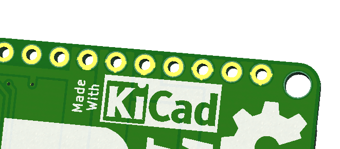
I gave a silly little “Intro to KiCad” presentation at our meetup last night, before the weather came and insisted we not congregate outdoors.
I shit you not, it happened almost too fast to document. “Oh look, the sky is threatening. Oh wow, the wind is picking up. Better get the electronics inside. Oh, there go the beer cans and a dessert plate. Holy shit.
Then everyone scattered home, and it really came down. We actually had hail. It was the first time hearing hail in our house. People were concerned. The cat was concerned.
Anyhow, I wanted to relay a problem/solution I ran across yesterday, because I hadn’t come across this particular solution to the problem in my Googling, and maybe this will help someone.
PROBLEM: When trying to do a 3D view, you get the dreaded “Cannot determine board outline” message and it will not properly render your board shape.
VARIANT 1: KiCad provides coordinates to look at. In most cases, this is because your board edges aren’t properly connected and locked together. Go around the perimeter, zoom in very close, and click both lines, observing where the square marking the end of the segment appears. If they are in the exact same point, they are locked together, move on to the next one. If you need to move one, move it until a circle with a square inside appears, that’s the locked/connected indicator while moving the line.
VARIANT 2: KiCad provides no further information, just the subject error message. This one took me a few minutes. I walked the perimeter and everything was fine/locked. I turned off all other layers’ visibility except for Edge Cuts and could see no stray segments. I was confused. So I went old school. Knowing that all of these files are just text files with information, I grepped the .kicad_pcb file for “Edge” and was treated with the following:
  (gr_line (start -189 84) (end -189 -90) (layer Edge.Cuts) (width 0.05))
  (gr_line (start -114 84) (end -189 84) (layer Edge.Cuts) (width 0.05))
  (gr_line (start -114 -90) (end -114 84) (layer Edge.Cuts) (width 0.05))
  (gr_line (start -189 -90) (end -114 -90) (layer Edge.Cuts) (width 0.05))
  (gr_line (start -151.86914 77.27188) (end -151.87168 77.27188) (layer Edge.Cuts) (width 0.05))
My first clue was that my board shape was a rectangle and there were five segments described. The second clue is that fifth segment was too short. Ridiculously short. Invisibly short. So I zoomed in at those coordinates, and sure enough, there was a stray dot of edge cut sitting there that couldn’t be seen without the zoom. I removed it, then everything was fine.
Documenting here in case it helps others. But if you don’t move your board outlines much, and don’t accidentally draw on the edge cut layer and forget it, this probably won’t happen to you.
It occurs to me that this happens frequently with other layers, I often end up with an extra dot of something that I discover later when zoomed in. It might be useful to have a routine or view that just highlights every sub-millimeter unnecessary portion of wire, mask, edge or silkscreen that was probably left there by accident. 🙂